B, Mini USB, 2.0, Receptacle, 5 Position, Top Mount, 1 Port, Right Angle, Tape & Reel, Flush, Surface Mount, Cable-to-Board
Industry: IoT & Embedded Systems
-
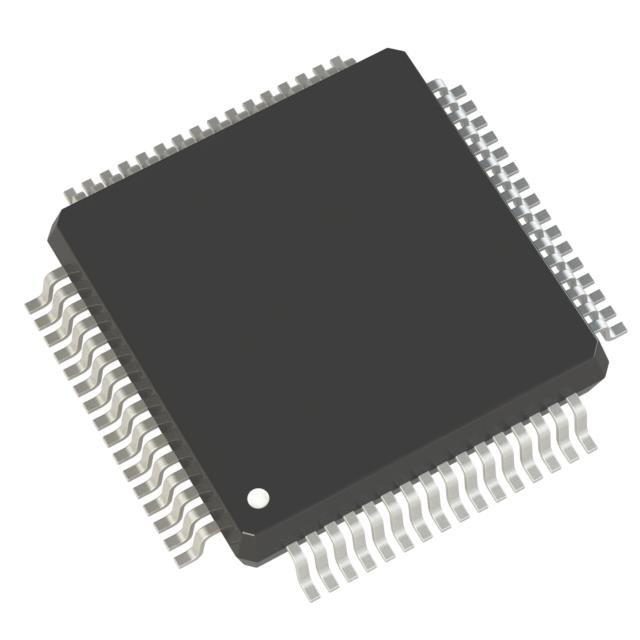
ATMEGA328P-AU
Port B is an 8-bit bi-directional I/O port with internal pull-up resistors (selected for each bit). The Port B output buffers have symmetrical drive characteristics with both high sink and source capability. As inputs, Port B pins that are externally pulled low will source current if the pull-up resistors are activated. The Port B pins are tristated when a reset condition becomes active, even if the clock is not running. Depending on the clock selection fuse settings, PB6 can be used as input to the inverting Oscillator amplifier and input to the internal clock operating circuit. Depending on the clock selection fuse settings, PB7 can be used as output from the inverting Oscillator amplifier. If the Internal Calibrated RC Oscillator is used as chip clock source, PB7…6 is used as TOSC2…1 input for the Asynchronous Timer/Counter2 if the AS2 bit in ASSR is set.
-
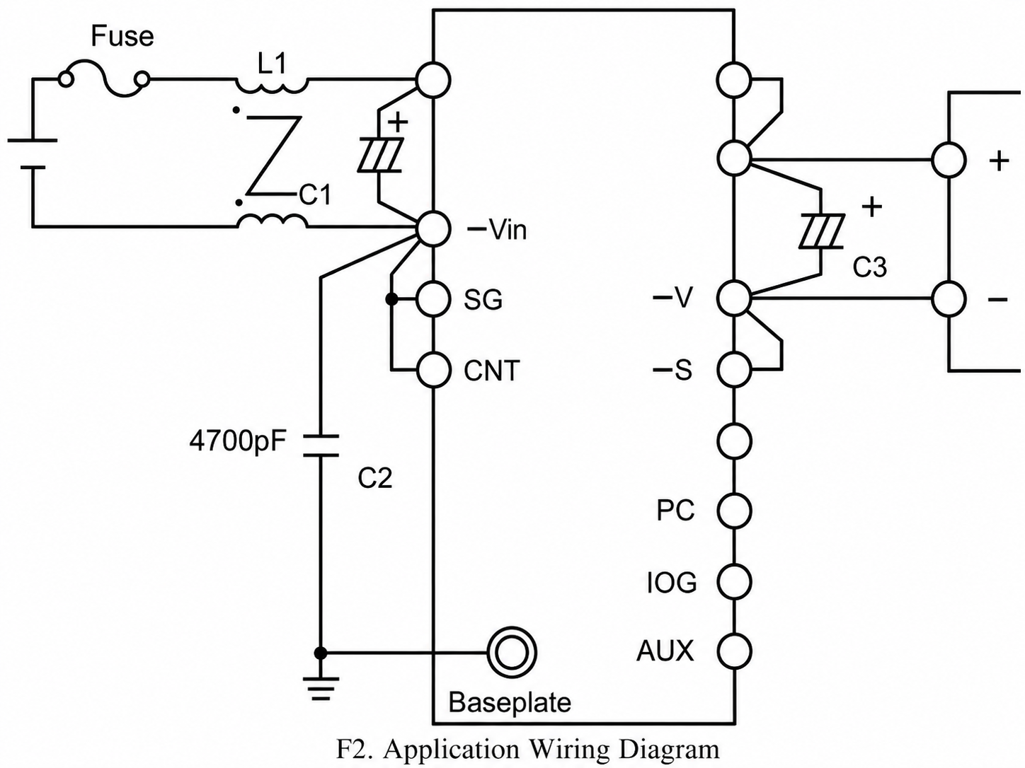
GCFCA2424S-100 100W Isolated DC/DC Converter | 18-36V Input | 24V 4.2A Output
GCFCA2424S-100 DC/DC Converter
The GCFCA2424S-100 is a high-performance isolated DC/DC converter designed for industrial power systems requiring reliable voltage conversion and electrical isolation. It operates from an 18V to 36V DC input and delivers a regulated 24V DC output with up to 4.2A output current and 100W output power.
The module incorporates advanced protection features including input under-voltage protection, output short-circuit protection, over-current protection, enable control, and parallel current sharing. With up to 88% efficiency and 2000VAC isolation, it is ideal for industrial automation, communication equipment, transportation systems, energy storage equipment, and distributed power architectures.
Applications
- Industrial automation systems
- Distributed power systems
- Telecommunication equipment
- Battery-powered equipment
- Transportation electronics
- Energy storage systems
- Power distribution equipment
- Embedded industrial control systems
-
GD25Q128CSIG
The GD25Q128C (128M-bit) Serial flash supports the standard Serial Peripheral Interface (SPI), and supports the
Dual/Quad SPI: Serial Clock, Chip Select, Serial Data I/O0 (SI), I/O1 (SO), I/O2 (WP#), and I/O3 (HOLD#/ RESET#).
The Dual I/O data is transferred with speed of 208Mbits/s and the Quad I/O & Quad output data is transferred with speed
of 320Mbits/s -
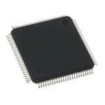
GD32E103VBT6
The GD32E103xx device belongs to the connectivity line of GD32 MCU Family. It is a 32-bit
general-purpose microcontroller based on the Arm® Cortex®-M4 RISC core with best costperformance ratio in terms of enhanced processing capacity, reduced power consumption
and peripheral set. The Cortex®-M4 core features implements a full set of DSP instructions to
address digital signal control markets that demand an efficient, easy-to-use blend of control
and signal processing capabilities. It also provides powerful trace technology for enhanced
application security and advanced debug support.
The GD32E103xx device incorporates the Arm® Cortex®-M4 32-bit processor core operating
at 120 MHz frequency with Flash accesses to obtain maximum efficiency. It provides up to
128 KB on-chip Flash memory and 32 KB SRAM memory. An extensive range of enhanced
I/Os and peripherals connected to two APB buses. The devices offer up to two 12-bit 3 MSPS
ADCs, two 12-bit DACs, up to ten general 16-bit timers, two 16-bit PWM advanced timers,
and two 16-bit basic timers, as well as standard and advanced communication interfaces: up
to three SPIs, two I2Cs, three USARTs and two UARTs, two I2Ss and an USBFS.
The device operates from 1.71 to 3.6 V power supply and available in –40 to +85 °C
temperature range. Several power saving modes provide the flexibility for maximum
optimization between wakeup latency and power consumption, an especially important
consideration in low power applications.
The above features make GD32E103xx devices suitable for a wide range of interconnection
and advanced applications, especially in areas such as industrial control, motor drives,
consumer and handheld equipment, human machine interface, security and alarm systems,
POS, automotive navigation, IoT and so on. -
LPC55S69JBD100
The LPC55S6x is an ARM Cortex-M33 based microcontroller for embedded applications. These devices include an ARM Cortex-M33 coprocessor, CASPER Crypto/FFT engine, PowerQuad hardware accelerator for DSP functions, up to 320 KB of on-chip SRAM, up to 640 KB on-chip flash, PRINCE module for on-the-fly flash encryption/decryption, high-speed and full-speed USB host and device interface with crystal-less operation for full-speed, SD/MMC/SDIO interface, five general-purpose timers, one SCTimer/PWM, one RTC/alarm timer, one 24-bit Multi-Rate Timer (MRT), a Windowed Watchdog Timer (WWDT), nine flexible serial communication peripherals (which can be configured as a USART, SPI, high speed SPI, I2C, or I2 S interface), Programmable Logic Unit (PLU), one 16-bit 1.0 Msamples/sec ADC capable of simultaneous conversions.
The ARM Cortex-M33 provides a security foundation, offering isolation to protect valuable IP and data with TrustZone® technology. It simplifies the design and software development of digital signal control systems with the integrated digital signal processing (DSP) instructions. To support security requirements, the LPC55S6x also offers support for secure boot, HASH, AES, RSA, UUID, DICE, dynamic encrypt and decrypt, debug authentication, and TBSA compliance.
-
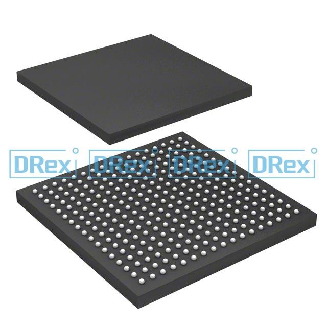
MCIMX6Y2CVM08AB (i.MX 6UL)
The i.MX 6ULL processors represent NXP’s latest achievement in integrated multimedia-focused products offering high performance processing with a high degree of functional integration, targeted towards the growing market of connected devices. The i.MX 6ULL is a high performance, ultra efficient processor family with featuring NXP’s advanced implementation of the single Arm Cortex®-A7 core, which operates at speeds of up to 792 MHz. i.MX 6ULL includes integrated power management module that reduces the complexity of external power supply and simplifies the power sequencing. Each processor in this family provides various memory interfaces, including LPDDR2, DDR3, DDR3L, Raw and Managed NAND flash, NOR flash, eMMC, Quad SPI, and a wide range of other interfaces for connecting peripherals, such as WLAN, Bluetooth™, GPS, displays, and camera sensors.
-
STM32L476RGT6
The STM32L476xx devices are ultra-low-power microcontrollers based on the high-performance Arm® Cortex®-M4 32-bit RISC core operating at a frequency of up to
80 MHz. The Cortex-M4 core features a Floating point unit (FPU) single precision that supports all Arm® single-precision data-processing instructions and data types. It also
implements a full set of DSP instructions and a memory protection unit (MPU) which enhances application security.The STM32L476xx devices embed high-speed memories (flash memory up to 1 Mbyte, up to 128 Kbyte of SRAM), a flexible external memory controller (FSMC) for static memories
(for devices with packages of 100 pins and more), a Quad SPI flash memories interface (available on all packages) and an extensive range of enhanced I/Os and peripherals
connected to two APB buses, two AHB buses and a 32-bit multi-AHB bus matrix. The STM32L476xx devices embed several protection mechanisms for embedded flash memory and SRAM: readout protection, write protection, proprietary code readout protection and Firewall.The devices offer up to three fast 12-bit ADCs (5 Msps), two comparators, two operational amplifiers, two DAC channels, an internal voltage reference buffer, a low-power RTC, two general-purpose 32-bit timer, two 16-bit PWM timers dedicated to motor control, seven general-purpose 16-bit timers, and two 16-bit low-power timers. The devices support four digital filters for external sigma delta modulators (DFSDM).
In addition, up to 24 capacitive sensing channels are available. The devices also embed an integrated LCD driver 8×40 or 4×44, with internal step-up converter. They also feature standard and advanced communication interfaces, namely three I2Cs, three SPIs, three USARTs, two UARTs and one Low-Power UART, two SAIs, one SDMMC, one CAN, one USB OTG full-speed, one SWPMI (single wire protocol master interface).
The STM32L476xx operates in the -40 to +85 °C (+105 °C junction), -40 to +105 °C (+125 °C junction) and -40 to +125 °C (+130 °C junction) temperature ranges from a 1.71 to 3.6 V VDD power supply when using internal LDO regulator and a 1.05 to 1.32V VDD12 power supply when using external SMPS supply. A comprehensive set of power-saving modes makes possible the design of low-power applications.
Some independent power supplies are supported: analog independent supply input for ADC, DAC, OPAMPs and comparators, 3.3 V dedicated supply input for USB and up to 14 I/Os can be supplied independently down to 1.08 V. A VBAT input makes it possible to backup the RTC and backup registers. Dedicated VDD12 power supplies can be used to bypass the internal LDO regulator when connected to an external SMPS. The STM32L476xx family offers seven packages from 64-pin to 144-pin packages
-
STM32MP157CAC3
The STM32MP157C/F devices are based on the high-performance dual-core Arm® Cortex®-A7 32-bit RISC core operating at up to 800 MHz. The Cortex-A7 processor includes a 32-Kbyte L1 instruction cache for each CPU, a 32-Kbyte L1 data cache for each CPU and a 256-Kbyte level2 cache. The Cortex-A7 processor is a very energy-efficient application processor designed to provide rich performance in high-end wearables, and other low-power embedded and consumer applications. It provides up to 20% more single thread performance than the Cortex-A5 and provides similar performance than the CortexA9.
The Cortex-A7 incorporates all features of the high-performance Cortex-A15 and CortexA17 processors, including virtualization support in hardware, NEON™, and 128-bit AMBA®4
AXI bus interface. The STM32MP157C/F devices also embed a Cortex® -M4 32-bit RISC core operating at up to 209 MHz frequency. Cortex-M4 core features a floating point unit (FPU) single precision which supports Arm® single-precision data-processing instructions and data types. The Cortex® -M4 supports a full set of DSP instructions and a memory protection unit (MPU)
which enhances application security. The STM32MP157C/F devices also embed a 3D graphic processing unit (Vivante® – OpenGL® ES 2.0) running at up to 533 MHz, with performances up to 26 Mtriangle/s, 133 Mpixel/s. The STM32MP157C/F devices provide an external SDRAM interface supporting external memories up to 8-Gbit density (1 Gbyte), 16 or 32-bit LPDDR2/LPDDR3 or DDR3/DDR3L up to 533 MHz. The STM32MP157C/F devices incorporate high-speed embedded memories with 708 Kbytes of Internal SRAM (including 256 Kbytes of AXI SYSRAM, 3 banks of 128 Kbytes each of AHB SRAM, 64 Kbytes of AHB SRAM in backup domain and 4 Kbytes of SRAM in backup domain), as well as an extensive range of enhanced I/Os and peripherals connected to APB buses, AHB buses, a 32-bit multi-AHB bus matrix and a 64-bit multi layer AXI interconnect supporting internal and external memories access.All the devices offer two ADCs, two DACs, a low-power RTC, 12 general-purpose 16-bit timers, two PWM timers for motor control, five low-power timers, a true random number generator (RNG), and a cryptographic acceleration cell. The devices support six digital filters for external sigma delta modulators (DFSDM). They also feature standard and advanced communication interfaces.
• Standard peripherals
– Six I2Cs
– Four USARTs and four UARTs
– Six SPIs, three I2Ss full-duplex master/slave. To achieve audio class accuracy, theI2S peripherals can be clocked via a dedicated internal audio PLL or via an external clock to allow synchronization.
– Four SAI serial audio interfaces
– One SPDIF Rx interface
– Management data input/output slave (MDIOS)
– Three SDMMC interfaces
– An USB high-speed Host with two ports two high-speed PHYs and a USB OTG high-speed with full-speed PHY or high-speed PHY shared with second port of USB Host.
– Two FDCAN interface, including one supporting TTCAN mode
– A Gigabit Ethernet interface
– HDMI-CEC• Advanced peripherals including
– A flexible memory control (FMC) interface
– A Quad-SPI flash memory interface
– A camera interface for CMOS sensors
– An LCD-TFT display controller
– A DSI Host interface.Refer to Table 1: STM32MP157C/F features and peripheral counts for the list of peripherals available on each part number. A comprehensive set of power-saving mode allows the design of low power applications. The STM32MP157C/F devices are proposed in 4 packages ranging from 257 to 448 balls with pitch 0.5 mm to 0.8 mm. The set of included peripherals changes with the device chosen. These features make the STM32MP157C/F suitable for a wide range of consumer, industrial, white goods and medical applications